Some physicists study stars in the sky, while some study electrons on earth. Stars are varied and colorful. Electrons, however, are indistinguishable, which give rise to the lonely story of one-electron universe.
A gate is a metal near an electron reservoir. By applying a voltage difference between the gate and the reservoir, electrons are transferred from one place to another. If the reservoir runs out of electrons, it becomes insulating. The door for current is then “closed” by the gate.
Sometimes a batch of very fine gates (<10nm) is needed for experiments. Here is a post sketching how to make a quantum nanowire device, with gates. These gates with <100 nm pitch can be made with either photolithography or e-beam lithography (EBL), or other methods. Academic people don’t care about mass production. They usually choose EBL, which is more flexible to use, with smaller de Broglie wavelength (thus smaller spot after well focused) while sacrifices the efficiency (the writing is done pixel by pixel).
EBL with 100 kV accelerating voltage is a high-end EBL. Here is an introduction to such an EBL. You can find tiny patterns they created with EBL on page 3 and 4 (20 nm period). But that it’s just the structure of the resist or a pattern transferred by etching. If you covered it with a metal, and do the “lift-off” process in order to wash the resist away and have a grating-gate left, you may get extra issues: The metal may be too sticky to get rid of, the resist is fully covered by metal and there is no way to be washed away, the yield is too low that you repeat a pattern for 1000 times and only one is good because of electron’s wave–particle duality… The sub-100 nm pitch gate is still not guaranteed even with a 100 kV EBL machine. You still need to think and practice.
One big problem for making sub-100 nm pitch dense gates is the proximity effect: electrons do not stay in a focused spot, instead, they go everywhere. You may make a long 10-nm-wide gold line on silicon easily, but feel difficult to repeat it for 100 times with 20 nm period at once. The proximity effect may cause the whole area to become a rectangle instead of lines after developing. The most straightforward way to make delicate patterns is to use the most dedicated EBL system, which has a 100 kV or higher e-beam. 30 kV e-beam is much worse than 100 kV in the aspect of proximity effect. However, it is more widely used in schools because it’s cheaper. And according to this paper, it is possible to make 60 nm pitch gratings with 3 kV e-beam (Fig. 19. Yes, it’s 3 kV, not 30 kV), and the resist after developed shows undercut features (Fig. 6) due to strong forward scattering, which is good for lift-off processes, amazing! But the window for 3 kV is very small (Fig. 7). It’s easier to work with a 30 kV e-beam, if 100 kV e-beam is not available, and with the trick of cold development. The cold development will significantly improve your EBL results. Another trick for EBL is that you can use IPA+water or even ethonal+water (=wine?) for development. They are less toxic and cheaper and better. If you don’t use them, you are “very much out of date”.
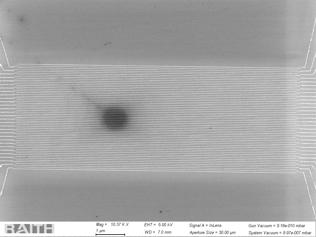
There’s an example of 60 nm pitch gates made with Raith e-LiNE (30 kV, developed at -15 C with MIBK:IPA 1:3). The mismatch between gates and outer leads looks like a Vernier scale. It is due to the fracturing of EBL system, which should be avoid. By default a polygon is fractured into lines parallel to its longest edge (whose angle changes gradually in this case) and the first few points in a line is not well exposed.